100GBASE-LR4 10km QSFP28 Transceiver
Model/PN: NASAQSFP100GLR4
Product Features
- • Hot-pluggable QSFP28 form factor
- • Supports 103.1Gb/s aggregate bit rate
- • Power dissipation < 3.5W
- • RoHS-6 compliant
- • Commercial case temperature range of 0°C to 70°C
- • Single 3.3V power supply
- • Maximum link length of 10km on Single Mode Fiber (SMF)
- • 4x26Gb/s EML-based LAN-WDM transmitter
- • 4x26G retimed electrical interface
- • Duplex LC receptacles
- • I2C management interface
Application
- • 100GBASE-LR4 100G Ethernet
1. Product Description
NASA-SI’s NASAQSFP100GLR4 QSFP28 transceiver modules are designed for use in 100 Gigabit Ethernet links on up to 10km of single mode fiber. They are individually tested on a series of Cisco, Juniper, Dell, HP, IBM…. switches, routers, servers, network interface card (NICs) etc, and is fully compliant with the QSFP28 MSA1, IEEE 802.3ba 100GBASE-LR42 and IEEE 802.3bm CAUI-46. Digital diagnostic functions are available via the I2C interface, as specified by the QSFP28 MSA. The transceiver is RoHS-6 compliant per Directive 2011/65/EC3.
2. Absolute Maximum Ratings
It has to be noted that the operation in excess of any individual absolute maximum ratings might cause permanent damage to this module.
|
Parameter |
Symbol |
Min |
Max |
Unit |
Note |
|
Storage Temperature Tst |
Tst |
40 |
+85 |
degC |
|
|
Relative Humidity (non-condensation) |
RH |
5 |
90 |
% |
|
|
Operating Case Temperature |
Topc |
-5 |
+75 |
degC |
|
|
Supply Voltage |
VCC |
-0.5 |
3.6 |
V |
|
3. Recommended Operating Conditions
|
Parameter |
Symbol |
Min. |
Typical |
Max. |
Unit |
|
Supply Voltage |
Vcc |
3.1 |
3.3 |
3.5 |
V |
|
Case Operating Temperature |
Tca |
5 |
25 |
75 |
ºC |
|
Data Rate Per Lane |
fd |
|
25.78125 |
|
Gbps |
|
Humidity |
Rh |
5 |
|
85 |
% |
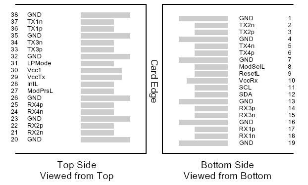
4. Pin Descriptions

|
Pin |
Symbol |
Name/Description |
Notes |
|
1 |
GND |
Ground |
1 |
|
2 |
Tx2n |
Transmitter Inverted Data Input |
|
|
3 |
Tx2p |
Transmitter Non-Inverted Data Input |
|
|
4 |
GND |
Ground |
1 |
|
5 |
Tx4n |
Transmitter Inverted Data Input |
|
|
6 |
Tx4p |
Transmitter Non-Inverted Data Input |
|
|
7 |
GND |
Ground |
1 |
|
8 |
ModSelL |
Module Select |
|
|
9 |
ResetL |
Module Reset |
|
|
10 |
Vcc Rx |
+3.3 V Power supply receiver |
|
|
11 |
SCL |
2-wire serial interface clock |
|
|
12 |
SDA |
2-wire serial interface data |
|
|
13 |
GND |
Ground |
1 |
|
14 |
Rx3p |
Receiver Non-Inverted Data Output |
|
|
15 |
Rx3n |
Receiver Inverted Data Output |
|
|
16 |
GND |
Ground |
1 |
|
17 |
Rx1p |
Receiver Non-Inverted Data Output |
|
|
18 |
Rx1n |
Receiver Inverted Data Output |
|
|
19 |
GND |
Ground |
1 |
|
20 |
GND |
Ground |
|
|
21 |
Rx2n |
Receiver Inverted Data Output |
|
|
22 |
Rx2p |
Receiver Non-Inverted Data Output |
|
|
23 |
GND |
Ground |
1 |
|
24 |
Rx4n |
Receiver Inverted Data Output |
|
|
25 |
Rx4p |
Receiver Non-Inverted Data Output |
|
|
26 |
GND |
Ground |
1 |
|
27 |
ModPrsL |
Module Present |
|
|
28 |
IntL |
Interrupt |
|
|
29 |
Vcc Tx |
+3.3 V Power supply transmitter |
|
|
30 |
Vcc1 |
+3.3 V Power Supply |
|
|
31 |
LPMode |
Low Power Mode |
|
|
32 |
GND |
Ground |
1 |
|
33 |
Tx3p |
Transmitter Non-Inverted Data Input |
|
|
34 |
Tx3n |
Transmitter Inverted Data Input |
|
|
35 |
GND |
Ground |
1 |
|
36 |
Tx1p |
Transmitter Non-Inverted Data Input |
|
|
37 |
Tx1n |
Transmitter Inverted Data Input |
|
|
38 |
GND |
Ground |
1 |
5. Electrical Characteristics (EOL, TOP = 0 to +70 C, VCC = 3.135 to 3.465 Volts)
|
Parameter |
Symbol |
Min |
Typ |
Max |
Unit |
Ref. |
|
Supply Voltage |
Vcc |
3.135 |
|
3.465 |
V |
|
|
Supply Current |
Icc |
|
|
1.12 |
A |
|
|
Module total power |
P |
|
|
3.5 |
W |
1 |
|
Transmitter |
||||||
|
Signaling rate per lane |
|
25.78125 ± 100 ppm |
GBd |
|
||
|
Differential data input swing per lane |
Vin,pp |
|
|
900 |
mV |
|
|
Differential input return loss (min) |
RLd(f) |
9.5 – 0.37f, 0.01≤f<8 4.75 – 7.4log10(f/14), 8 ≤f<19 |
dB |
|
||
|
Differential to common mode input return loss (min) |
RLdc(f) |
22-20(f/25.78), 0.01≤f<12.89 15-6(f/25.78), 12.89≤f<19 |
dB |
|
||
|
Differential termination mismatch |
|
|
|
10 |
% |
|
|
Stressed input parameters |
|
|
|
|
|
|
|
Eye width |
|
|
0.46 |
|
UI |
|
|
Applied pk-pk sinusoidal jitter |
|
Per IEEE 802.3bm Table 88-13 |
|
|
||
|
Eye height |
|
|
95 |
|
mV |
|
|
DC common mode voltage |
|
-350 |
|
2850 |
mV |
|
|
Receiver |
||||||
|
Signaling rate per lane |
|
25.78125 ± 100 ppm |
GBd |
|
||
|
Differential data output swing |
Vout,pp |
100 |
|
400 |
mVpp |
2 |
|
300 |
|
600 |
||||
|
400 |
|
800 |
||||
|
600 |
|
1200 |
||||
|
Eye width |
|
0.57 |
|
|
UI |
|
|
Vertical eye closure |
|
|
|
5.5 |
dB |
|
|
Differential output return loss (min) |
RLd(f) |
9.5 – 0.37f, 0.01≤f<8 4.75 – 7.4log10(f/14), 8 ≤f<19 |
dB |
|
||
|
Common to differential mode conversion return loss (min) |
RLdc(f) |
22-20(f/25.78), 0.01≤f<12.89 15-6(f/25.78), 12.89≤f<19 |
dB |
|
||
|
Differential termination mismatch |
|
|
|
10 |
% |
|
|
Transition time, 20% to 80% |
tr tf |
12 |
|
|
ps |
|
Notes:
- Maximum total power value is specified across the full temperature and voltage range.
- Output voltage is settable in 4 discrete ranges via I2C. Default range is 400 – 800 mV.
6. Optical Characteristics (EOL, TOP = 0 to +70 C, VCC = 3.135 to 3.465 Volts)
|
Parameter |
Symbol |
Min |
Typ |
Max |
Unit |
Ref. |
|
Transmitter |
||||||
|
Signaling Speed per Lane |
|
25.78125 ± 100 ppm |
Gb/s |
1 |
||
|
Lane center wavelengths (range) |
|
1294.53 – 1296.59 1299.02 – 1301.09 1303.54 – 1305.63 1308.09 – 1310.19 |
nm |
|
||
|
Total Average Launch Power |
POUT |
|
|
10.5 |
dBm |
|
|
Transmit OMA per Lane |
TxOMA |
-1.3 |
|
4.5 |
dBm |
|
|
Average Launch Power per Lane |
TXPx |
-4.3 |
|
4.5 |
dBm |
2,7 |
|
Optical Extinction Ratio |
ER |
4 |
|
|
dB |
|
|
Sidemode Suppression ratio |
SSRmin |
30 |
|
|
dB |
|
|
Average launch power of OFF transmitter, per lane |
|
|
|
-30 |
dBm |
|
|
Relative Intensity Noise |
RIN |
|
|
-130 |
dB/Hz |
|
|
Optical Return Loss Tolerance |
|
|
|
20 |
dB |
|
|
Transmitter Reflectance |
|
|
|
-12 |
dB |
|
|
Transmitter eye mask definition {X1, X2, X3, Y1, Y2, Y3} |
|
{0.25, 0.4, 0.45, 0.25, 0.28, 0.4} |
|
3 |
||
|
Receiver |
||||||
|
Signaling Speed per Lane |
|
25.78125 ± 100 ppm |
GBd |
4 |
||
|
Lane center wavelengths (range) |
|
1294.53 – 1296.59 1299.02 – 1301.09 1303.54 – 1305.63 1308.09 – 1310.19 |
nm |
|
||
|
Receive Power (OMA) per Lane |
RxOMA |
|
|
4.5 |
dBm |
|
|
Average Receive Power per Lane |
RXPx |
-10.6 |
|
4.5 |
dBm |
5,7 |
|
Receiver Sensitivity (OMA) per Lane |
Rxsens |
|
|
-8.6 |
dBm |
|
|
Return Loss |
RL |
-26 |
|
|
dB |
|
|
Stressed Receiver Sensitivity (OMA) per Lane |
SRS |
|
|
-6.8 |
dBm |
6 |
|
Receive electrical 3 dB upper cutoff frequency, per lane |
|
|
|
31 |
GHz |
|
|
LOS De-Assert |
LOSD |
|
|
-11.6 |
dBm |
|
|
LOS Assert |
LOSA |
-24 |
|
-13.6 |
dBm |
|
|
LOS Hysteresis |
|
|
1.5 |
|
dBm |
|
Notes:
- Transmitter consists of 4 lasers operating at 25.78Gb/s each.
- Minimum value is informative.
- Hit ratio 5×10⁻⁵.
- Receiver consists of 4 photodetectors operating at 25.78Gb/s each.
- Minimum value is informative, equals min TxOMA with infinite ER and max channel insertion loss.
- SRS is measured with vertical eye closure penalty of 1.8 dB max, J2 of 0.30 UI, and J9 of 0.47 UI.
- Power value and power accuracy are with all channels on.
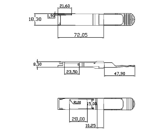
7. Mechanical Specifications

8. ESD
This transceiver is specified as ESD threshold 1kV for all electrical input pins, tested per MIL-STD-883, Method 3015.4 /JESD22-A114-A (HBM). However, normal ESD precautions are still required during the handling of this module. This transceiver is shipped in ESD protective packaging. It should be removed from the packaging and handled only in an ESD protected environment.
9. Laser Safety
This is a Class 1 Laser Product according to IEC 60825-1:1993:+A1:1997+A2:2001. This product complies with 21 CFR 1040.10 and 1040.11 except for deviations pursuant to Laser Notice No. 50, dated (July 24, 2007).
Ordering Information
|
Part Number |
Product Description |
|
NASAQSFP100GLR4 |
100Gbps QSFP28, 850nm,100m, -5℃~+75℃ |
VERSION UPDATE:
|
VERSION NO. |
DATE |
UPDATED INFORMATION |
|
V20151101 |
20151101 |
1. NEW PUBLISHED |
NOTICE: NASA-SI reserves the right to make changes to this product in this specification without notice, in order to improve product performance.


