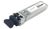
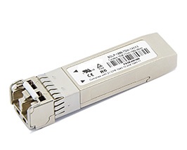
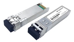
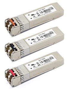
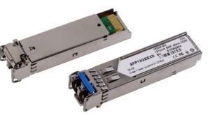
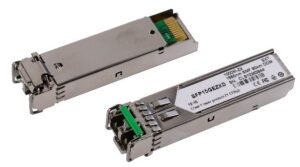
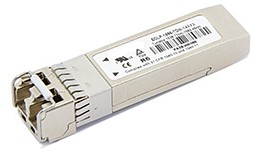
25.78Gbps 100m SFP+ Transceiver
Model/PN: NASASFPP25GSR
Features
- • Supports 25GBASE-SR(25Gb/s);
- • Lane bit rate 25.78 Gb/s;
- • Maximum link length of 70m on OM3 MMF and 100m on OM4 MMF;
- • 850nm VCSEL laser and PIN photo-detector;
- • High speed I/O electrical interface (25GAUI);
- • I2C interface with integrated Digital Diagnostic monitoring;
- • SFP28 MSA package with duplex LC connector;
- • Maximum power consumption 1.0W
- • Single +3.3V power supply;
- • Operating case temperature: Refer to Order info.
- • Compliant to IEEE 802.3cc Draft3.0, SFF-8402 and SFF-8432;
- • Complies with EU Directive 2011/65/EU (RoHS 6/6);
Application
- • 25GBase-SR
- • CPRI
1. Product Description
NASASFPP25GSR compatible SFP28 transceiver adopts LC duplex connectors, reaching a link up to 100m over OM4 MMF (70m over OM3). The SFP28 transceiver module supports running on the same 1G/10G network cabling Infrastructure, giving 2.5 times increase in speed at least, and the built-in DDM/DOM functions monitor the real-time operating status. Each SFP28 transceiver module is individually tested on a series of Cisco, Juniper, Dell, HP, IBM…. switches, routers, servers, network interface card (NICs) etc, and is fully compliant with the SFP28 MSA, RoHS, CPRI, and the eCPRI standards. Featuring low power consumption, high speed, this 25G transceiver is ideal for 25G Ethernet, telecom, and data center.
2. Absolute Maximum Ratings
|
Parameter |
Symbol |
Min. |
Typical |
Max. |
|
Storage Temperature |
TS |
-40 |
– |
+85 |
|
Supply Voltage |
VCC |
-0.5 |
– |
+4.0 |
|
Operating Relative Humidity |
RH |
– |
– |
+85 |
3. Recommended Operating Conditions
|
Parameter |
Symbol |
Min. |
Typical |
Max. |
Unit |
|
Operating Case Temperature NASASFP25GSR |
TC |
-5 |
– |
+70 |
°C |
|
Operating Case Temperature NASASFP25GSRI |
TC |
-40 |
– |
+85 |
°C |
|
Power Supply Voltage |
VCC |
3.13 |
3.3 |
3.47 |
V |
|
Power Supply Current |
ICC |
– |
– |
0.28 |
A |
|
Maximum Power Dissipation |
PD |
– |
– |
1.0 |
W |
|
Lane Bit Rate |
BRLANE |
24.3 |
25.78 |
26.5 |
Gb/s |
|
Transmission Distance(OM3) |
TD |
|
|
70 |
m |
|
Transmission Distance(OM4) |
TD |
|
|
100 |
m |
4. Optical Characteristics
|
Transmitter |
||||||
|
Parameter |
Symbol |
Min. |
Typical |
Max. |
Unit |
Notes |
|
Center Wavelength |
λ0 |
840 |
850 |
860 |
nm |
|
|
Average Launch Power |
PTX_LANE |
-8.4 |
– |
2.4 |
dBm |
1 |
|
Optical Modulation Amplitude |
OMA |
-6.4 |
– |
3 |
dBm |
|
|
Launch power in OMA minus TDP (min) |
OMA_TDP |
-7.3 |
– |
– |
dBm |
|
|
Difference in launch power between lanes |
PTX_DELTA_LANE |
– |
– |
3.6 |
dB |
|
|
Average Output Power (Laser Turn off) |
P0UT-OFF |
– |
– |
-30 |
dBm |
|
|
Extinction Ratio |
ER |
2 |
– |
– |
dB |
|
|
Transmitter and dispersion penalty (TDP) |
TDP |
– |
– |
4.3 |
dB |
|
|
Optical Return Loss Tolerance |
ORLT |
– |
– |
12 |
dB |
|
|
Optical Eye Mask |
Compliant with IEEE 802.3cc Draft 3.0 |
|
||||
|
Receiver |
||||||
|
Center Wavelength |
λ0 |
840 |
850 |
860 |
nm |
|
|
Average Rx Power per Lane, 100GE |
PRX _LANE |
-10.3 |
– |
2.4 |
dBm |
2 |
|
Receiver sensitivity (OMA) |
POMA_LANE |
– |
– |
-5.2 |
dBm |
2 |
|
Receiver Overload |
PIN-OL |
3.4 |
– |
– |
dBm |
|
|
Reflectance |
Ref |
– |
– |
-12 |
dB |
|
|
LOS Assert per lane |
LOSA |
-30 |
– |
– |
dBm |
|
|
LOS De-assert |
LOSD |
– |
– |
-17 |
dBm |
|
|
LOS Hysteresis |
LOSH |
0.5 |
– |
4 |
dB |
|
Notes:
- Class 1 Laser Safety limit per FDA/CDRH, and EN (IEC) 60825 laser safety standards.
- Informative Only
5. Electrical Characteristics
|
Transmitter (Module Input) |
|||||||
|
Parameter |
Symbol |
Min. |
Typical |
Max. |
Unit |
Notes |
|
|
Differential Data Input Amplitude |
VIN,P-P |
90 |
– |
800 |
mVpp |
|
|
|
Differential Termination Mismatch |
|
– |
– |
5 |
% |
|
|
|
Tx_Disable |
Normal Operation |
VIL |
-0.3 |
– |
0.8 |
V |
|
|
Laser Disable |
VIH |
2.0 |
– |
VCC+0.3 |
V |
|
|
|
Receiver (Module Output) |
|||||||
|
Differential Data Output Amplitude |
VOUT,P-P |
185 |
– |
425 |
mVpp |
|
|
|
Differential Termination Mismatch(1MHZ) |
|
– |
– |
5 |
% |
|
|
|
Output Rise/Fall Time, 20%~80% |
TR |
12 |
– |
– |
ps |
|
|
|
Rx_LOS |
Normal Operation |
VOL |
– |
– |
0.2 |
V |
|
|
Lose Signal |
VOH |
VCC-0.2 |
– |
– |
V |
|
|
6. Pin Description
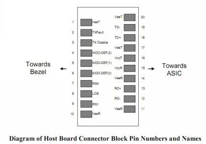
|
Pin |
Symbol |
Description |
Ref. |
|
1 |
VEET |
Transmitter Ground (Common with Receiver Ground) |
7.1 |
|
2 |
TFAULT |
Transmitter Fault. Not supported. |
|
|
3 |
TDIS |
Transmitter Disable. Laser output disabled on high or open. |
7.2 |
|
4 |
MOD_DEF(2) |
Module Definition 2. Data line for Serial ID. |
7.3 |
|
5 |
MOD_DEF(1) |
Module Definition 1. Clock line for Serial ID. |
7.3 |
|
6 |
MOD_DEF(0) |
Module Definition 0. Grounded within the module. |
7.3 |
|
7 |
RS0 |
Rate Select0, optionally controls SFP+ module receiver. When high input signaling rate>4.25 GBd and when low input signaling rate<4.25GBd |
|
|
8 |
LOS |
Loss of Signal indication. Logic 0 indicates normal operation. |
7.4 |
|
9 |
RS1 |
Rate Select1, optionally controls SFP+ module receiver. When high input signaling rate>4.25 GBd and when low input signaling rate<4.25GBd |
|
|
10 |
VEER |
Receiver Ground (Common with Transmitter Ground) |
7.1 |
|
11 |
VEER |
Receiver Ground (Common with Transmitter Ground) |
7.1 |
|
12 |
RD- |
Receiver Inverted DATA out. AC Coupled. |
|
|
13 |
RD+ |
Receiver Non-inverted DATA out. AC Coupled. |
|
|
14 |
VEER |
Receiver Ground (Common with Transmitter Ground) |
7.1 |
|
15 |
VCCR |
Receiver Power Supply |
|
|
16 |
VCCT |
Transmitter Power Supply |
|
|
17 |
VEET |
Transmitter Ground (Common with Receiver Ground) |
7.1 |
|
18 |
TD+ |
Transmitter Non-Inverted DATA in. AC Coupled. |
|
|
19 |
TD- |
Transmitter Inverted DATA in. AC Coupled. |
|
|
20 |
VEET |
Transmitter Ground (Common with Receiver Ground) |
7.1 |
Notes:
1 Circuit ground is internally isolated from chassis ground.
2 Laser output disabled on TDIS >2.0V or open, enabled on TDIS <0.8V.
3 Should be pulled up with 4.7k – 10kohms on host board to a voltage between 2.0V and 3.6V. MOD_DEF(0) pulls line low to indicate module is plugged in.
4 LOS is open collector output. Should be pulled up with 4.7k -10kohms on host board to a voltage between 2.0V and 3.6V. Logic 0 indicates normal operation; logic 1 indicates loss of signal.
7. EEPROM & DDM THRESHOLD
7.1 EEPROM
2 wire address 1010000X (A0h)
|
0~95 Serial ID Defined by SFP MSA (96 bytes) |
|
96~127 Vendor Specific (32 bytes) |
|
128~255 Reserved (128 bytes) |
7.2 DDM THRESHOLD
|
|
Low Alarm |
Low Warn |
High Warn |
High Alarm |
|
Temperature NASASFP25GSR |
-10℃ |
-5℃ |
70℃ |
75℃ |
|
Voltage |
3V |
3.1V |
3.5V |
4V |
|
Tx Bias |
2mA |
3mA |
10mA |
11mA |
|
Tx Power |
-9dBm |
-6dBm |
3dBm |
3.5dBm |
|
Rx Power |
-13dBm |
-10dBm |
3dBm |
3.5dBm |
8. Mechanical Specifications
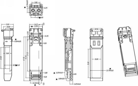
9. Label
NASA-SI offers label OEM design and print.
Label barcode supports code128 and 2D barcode
SIZE: 26mm*10.5mm
10. Warnings
Handling Precautions: This device is susceptible to damage as a result of electrostatic discharge (ESD). A static free environment is highly recommended. Follow guidelines according to proper ESD procedures.
Laser Safety: Radiation emitted by laser devices can be dangerous to human eyes. Avoid eye exposure to direct or indirect radiation.
11. Order Information
|
Part No. |
Data Rate |
Laser |
Fiber Type |
Distance |
Optical Interface |
Temp |
DDMI |
|
NASASFPP25GSR |
25.78Gbps |
850nm |
MMF |
100m |
LC |
-5~70 °C |
Y |
VERSION UPDATE:
|
VERSION NO. |
DATE |
UPDATED INFORMATION |
|
V20160818 |
20160818 |
1. EEPROM& DDM Threshold updated 2. “LABEL” added 3. Ordering information updated 4. Product picture updated |
NOTICE: NASA-SI reserves the right to make changes to this product in this specification without notice, in order to improve product performance.

