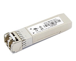
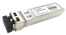
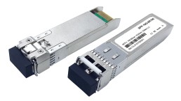
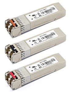
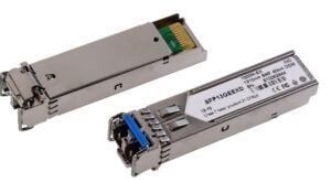
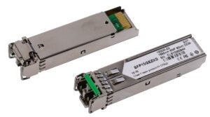
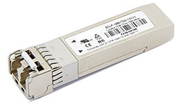
1.25G 850nm 550m SFP Transceiver
Model/PN: NASASFP850GESR
Product Features
- • Dual data-rate of 1.25Gbps operation
- • 850nm VCSEL laser and PIN photodetector
- • Compliant with SFP MSA and SFF-8472
- • 500m transmission with 50/125µm MMF
- • 300m transmission with 62.5/125µm MMF
- • Duplex LC Receptacle
- • Hot-pluggable SFP footprint
- • Single 3.3V power supply
- • All-metal housing for superior EMI performance
- • Operating temperature 0 ~ 70oC
- • BER ≤ 10-12.
- • Digital Diagnostic Monitor (DDM)
Applications
- • 1.25Gbps 1000Base-LX IEEE 802.3z
- • CPRI/OBSAI Fiber Channel
- • Switch to Switch Interface
- • Switched backplane application
- • Router/Server interface
- • BTS application
- • Other Optical transmission system
1. Product Description
The NASASFP850GESR are small form factor pluggable (SFP) transceiver module is individually tested on a series of Cisco, Juniper, Dell, HP, SIENA…. switches, routers, servers, network interface card (NICs), BTS of Huawei, Ericsson, Nokia, etc. and is fully compatible with multi-sourcing agreement (MSA). It is suitable for multi-mode fiber (MMF) communications in 1.25Gbps Ethernet and CPRI/OBSAI Fiber Channel.
The SFP transceiver is high performance, cost effective modules supporting data-rate of 1.25Gbps and 550m transmission distance with MMF.
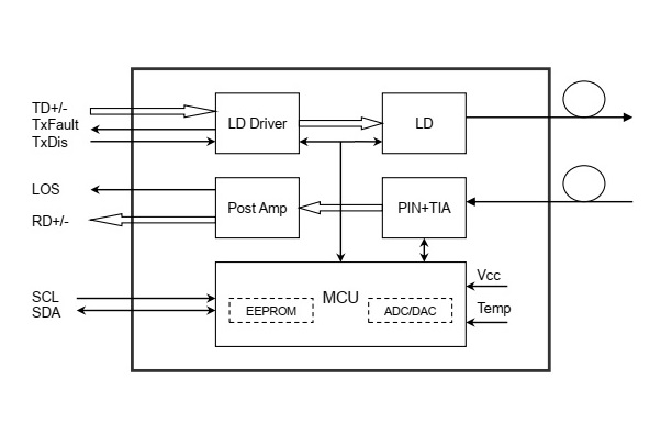
The transceiver consists of three sections: a VCSEL laser transmitter, a PIN photodiode integrated with a trans-impedance preamplifier (TIA) and MCU control unit. All modules satisfy class I laser safety requirements.
The transceivers are compatible with SFP Multi-Source Agreement (MSA) and SFF-8472. For further information, please refer to SFP MSA.
2. Regulatory Compliance
NASA-SI transceivers are Class 1 Laser Products comply with FDA regulations. Meet Class 1 eye safety requirements of EN 60825 and the electrical safety requirements of EN 60950.
3. Absolute Maximum Ratings
|
Parameter |
Symbol |
Min. |
Max. |
Unit |
|
Supply Voltage |
Vcc |
-0.5 |
4.5 |
V |
|
Storage Temperature |
Ts |
-40 |
85 |
°C |
|
Relative Humidity |
RH |
5 |
85 |
% |
4. Recommended Operating Conditions
|
Parameter |
Symbol |
Min. |
Typical |
Max. |
Unit |
|
Power Supply Voltage |
Vcc |
3.13 |
3.3 |
3.47 |
V |
|
Power Supply Current |
Icc |
|
|
300 |
mA |
|
Operating Case Temperature |
Tc |
0 |
|
70 |
oC |
|
Data Rate, Gigabit Ethernet |
|
|
1.25 |
|
Gbps |
5. Optical Characteristics
|
Parameter |
Symbol |
Min. |
Typical |
Max. |
Unit |
Note |
|
Transmitter |
|
|||||
|
Centre Wavelength |
λc |
830 |
850 |
860 |
nm |
|
|
Spectral Width (RMS) |
σ |
|
|
0.85 |
nm |
|
|
Average Output Power |
Pout |
-9.5 |
|
-3 |
dBm |
Note 1 |
|
Extinction Ratio |
ER |
9 |
|
|
dB |
|
|
Optical Rise/Fall Time (20% to 80%) |
tr/tf |
|
|
0.26 |
ns |
|
|
Receiver |
|
|||||
|
Centre Wavelength |
λc |
770 |
|
860 |
nm |
|
|
Receiver Sensitivity |
PIN |
|
|
-19 |
dBm |
Note 2 |
|
Receiver Overload |
Pmax |
-3 |
|
|
dBm |
Note 2 |
|
LOS De-Assert |
LOSD |
|
|
-20 |
dBm |
|
|
LOS Assert |
LOSA |
-30 |
|
|
dBm |
|
|
LOS Hysteresis |
|
1 |
|
4 |
dB |
|
Notes:
- The optical power is launched into SMF.
- Measured with a PRBS 27-1 test pattern > 1250Mbps, BER ≤ 10-12.
6. Electrical Characteristics
|
Parameter |
Symbol |
Min. |
Typical |
Max. |
Unit |
Note |
|
Transmitter |
|
|||||
|
Input Differential Impedance |
Zin |
90 |
100 |
110 |
Ω |
|
|
Data Input Swing Differential |
Vin |
400 |
|
1800 |
mV |
Note 1 |
|
Tx-Dis Disable |
Vd |
2.0 |
|
Vcc |
V |
|
|
Tx-Dis Enable |
Ven |
0 |
|
0.8 |
V |
|
|
TX-Fault (Fault) |
|
2.0 |
|
Vcc |
V |
|
|
TX-Fault (Normal) |
|
0 |
|
0.8 |
V |
|
|
Receiver |
|
|||||
|
Data Output Swing Differential |
Vout |
400 |
|
1800 |
mV |
Note 2 |
|
Rx-Los High |
Vhi |
2.0 |
|
Vcc |
V |
|
|
Rx-Los Low |
Vlo |
0 |
|
0.8 |
V |
|
Notes:
- PECL input, internally AC-coupled and terminated.
- Internally AC-Coupled
7. Pin Descriptions
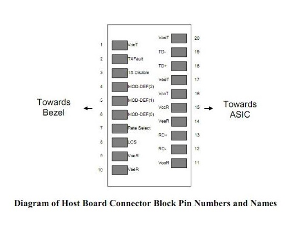
|
Pin |
Symbol |
Description |
Note |
|
1 |
VEET |
Transmitter Ground (Common with Receiver Ground) |
|
|
2 |
TX FAULT |
Transmitter Fault. Not supported. |
Note 1 |
|
3 |
TX DISABLE |
Transmitter Disable. Laser output disabled on high or open. |
Note 2 |
|
4 |
MOD_DEF(2) |
SDA Serial Data Signal |
Note 3 |
|
5 |
MOD_DEF(1) |
SCL Serial Clock Signal |
Note 3 |
|
6 |
MOD_DEF(0) |
Module Definition 0. Grounded within the module. |
Note 3 |
|
7 |
Rate Select |
Not Connected |
|
|
8 |
LOS |
Loss of Signal |
Note 4 |
|
9 |
VEER |
Receiver Ground |
|
|
10 |
VEER |
Receiver Ground |
|
|
11 |
VEER |
Receiver Ground |
|
|
12 |
RD- |
Receiver Inverted DATA out. |
Note 5 |
|
13 |
RD+ |
Receiver DATA out. |
Note 5 |
|
14 |
VEER |
Receiver Ground |
|
|
15 |
VCCR |
Receiver Power Supply |
|
|
16 |
VCCT |
Transmitter Power Supply |
|
|
17 |
VEET |
Transmitter Ground |
|
|
18 |
TD+ |
Transmitter DATA in. |
Note 6 |
|
19 |
TD- |
Transmitter Inverted DATA in. |
Note 6 |
|
20 |
VEET |
Transmitter Ground (Common with Receiver Ground) |
|
Notes:
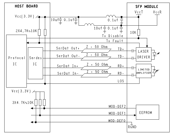
- TX Fault is an open collector output, which should be pulled up with a 4.7k~10kΩ resistor on the host board to a voltage between 2.0V and Vcc+0.3V. Logic 0 indicates normal operation; Logic 1 indicates a laser fault of some kind. In the low state, the output will be pulled to less than 0.8V.
- TX Disable is an input that is used to shut down the transmitter optical output. It is pulled up within the module with a 4.7k~10kΩ resistor. Its states are:
Low (0 to 0.8V): Transmitter on
(>0.8V, < 2.0V): Undefined
High (2.0 to 3.465V): Transmitter Disabled
Open: Transmitter Disabled
- Mod-Def 0,1,2. These are the module definition pins. They should be pulled up with a 4.7k~10kΩ resistor on the host board. The pull-up voltage shall be VccT or VccR.
Mod-Def 0 is grounded by the module to indicate that the module is present
Mod-Def 1 is the clock line of two wire serial interface for serial ID
Mod-Def 2 is the data line of two wire serial interface for serial ID
- LOS is an open collector output, which should be pulled up with a 4.7k~10kΩ resistor. Pull up voltage between 2.0V and Vcc+0.3V. Logic 1 indicates loss of signal; Logic 0 indicates normal operation. In the low state, the output will be pulled to less than 0.8V.
- RD-/+: These are the differential receiver outputs. They are internally AC-coupled 100 differential lines which should be terminated with 100Ω (differential) at the user SERDES.
- TD-/+: These are the differential transmitter inputs. They are internally AC-coupled, differential lines with 100Ω differential termination inside the module.
8. Digital Diagnostic Memory Map
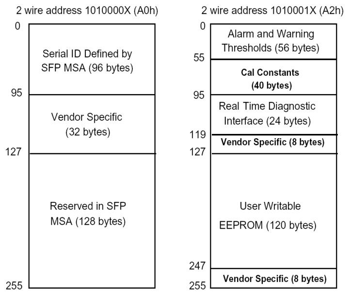
The transceivers provide serial ID memory contents and diagnostic information about the present operating conditions by the 2-wire serial interface (SCL, SDA).
The diagnostic information with internal calibration or external calibration all are implemented, including received power monitoring, transmitted power monitoring, bias current monitoring, supply voltage monitoring and temperature monitoring.
The digital diagnostic memory map specific data field defines as following.
9. Recommendation Circuit
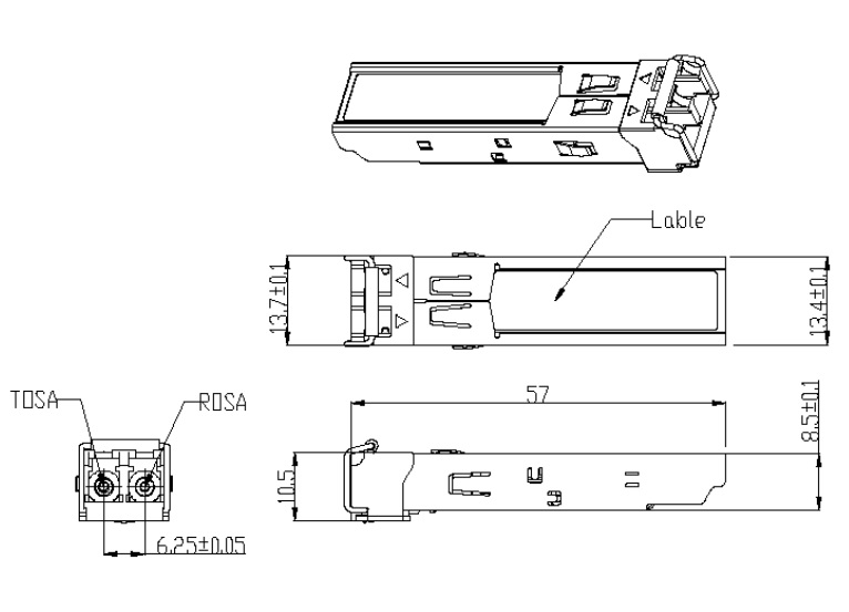
10. Mechanical Specifications
Ordering Information
|
Part No. |
Data Rate |
DDM |
Wave |
Fiber Type |
Dist. |
Temp. |
Optical Interface |
|
NASASFP850GESR |
1.25Gbps |
Yes |
850nm |
MMF |
550m |
0~70℃ |
LC |
Version Update:
|
VERSION NO. |
DATE |
UPDATED INFORMATION |
|
V20161010 |
20161010 |
1. EEPROM& DDM Threshold updated 2. “LABEL” added 3. Ordering information updated 4. Product picture updated |
|
V20170819 |
20170819 |
1. Ordering information updated |
NOTICE: NASA-SI reserves the right to make changes to this product in this specification without notice, in order to improve product performance.


